CAN Link Part 4

After finishing up another project this week, I realized that arbitrary dimensions I picked for it fit inside the dimensions of the CAN Link project.

I spent a bit of time mocking the i.MX6 device up on the PCB and it fit really well. The width of both PCBs just happened to be the same. This will make porting the device to the i.MX platform really easy assuming the devboard actually works. I didn’t want to actually finalize this design yet because I still don’t know if the new circuit actually works.
What I did realize during this exercise however, is that all the components that are common between both designs would not need to move at all. I could even separate the design into two separate PCBS!

So I started scheming on changes to the top half of the board. I figured there must be a suitable way to connect two PCBs horizantally. This was surprisingly difficult to find in a way that didn’t look really ugly. (yeah; that was the primary deciding factor)
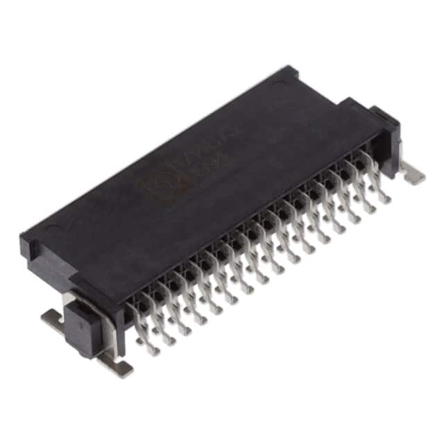
The coolest part about this component is that it’s a pretty “standard” pin spacing meaning a 1.27mm socket fits in place of this locking connector

Since this was mostly just a job of removing a lot of components, I didnt have much else to do here other than plumb up the new connector. Most of the signals were already going through this route anyway; I just terminated them, sliced the board in half and it was pretty much done. I sprinkled some silkscreen indicating what each pin does and got to prepping for fabrication. I was planning on having JLCPCB assemble the board, but none of difficult to solder components are basic parts. I had them fabricate it for a grand total of $38. Once my i.MX 6 board is confirmed functioning, I’ll be designing the bottom half of this board. Ideally “design” is used lightly here, it should be really simple.

